X-ray inspection of BGA and CSP for missing, shorts, voids, and junction condition
X-ray inspection of BGA (Ball Grid Array) and CSP (Chip Scale Package) is one of the non-destructive inspection methods to evaluate the solder joint condition. This inspection method uses X-ray images of the solder joint condition between the BGA or CSP and the printed circuit board (PCB) to detect defects such as ball position, shape, bridge, non-wet open, crack, and void.
X-ray inspection is used in PCB surface mount technology because it is impossible to check the joint position and condition of the hidden bottom terminals of BGAs and CSPs. As semiconductor packages become smaller and denser, X-ray inspection with high magnification and high accuracy is required, and microfocus X-ray inspection systems can meet the demand.
BGA X-ray inspection items
Bridging, non-wet open, void, no bump, no pad, no solder, misalignment, tilt, bump size


X-ray inspection of IC and LED wire bonding breaks, poor connections, and wire flow
Checking the wire bonding status of semiconductors such as ICs and LEDs is essential for improving the reliability of electronic components and electronic equipment. Matsusada Precision's X-ray inspection systems are ideal for checking minute wire breaks, connection defects in electronic devices such as ICs and LEDs, and an absence of wire flow.


X-ray inspection of the winding condition of batteries and capacitors
Matsusada Precision's X-ray non-destructive inspection systems are available for inspecting defects that could cause critical damage to the performance, such as the winding condition of battery electrode plates and electrolytic paper and electrode foil of capacitors without destroying the inspection parts.


Inspection of mounting and solder void conditions of power devices such as IGBTs and power MOSFETs, IC chips, etc
For IGBT (Insulated-Gate Bipolar Transistor), IPM (Intelligent Power Module), SiC and GaN power semiconductors, packaging and mounting techniques require inspection of the void fraction at joints, including heat dissipation performance. One semiconductor supplier requires solder joints to be mounted with a void ratio of under 25%.
In surface mount technology for power devices, accurate control of solder joints in terms of void ratio and solder quantity by X-ray inspection is essential.
Semiconductor packaging and mounting requiring accurate void measurement at critical solder joint interfaces
- LGA (Land Grid Array)
- QFN (Quad Flat No Leads)
- COB (Chip On Board)
- DBC (Direct Bonded Copper) Substrate
- AMB (Active metal brazed) Substrate

X-ray inspection of relay and switch contact conditions
Our X-ray non-destructive inspection systems are used to find out the cause of switch malfunction. It detects disconnection, contact fusion, melting, or welding. It is also available to detect contact instability caused by the deformation of the internal components due to external shocks.


X-ray inspection of the state of the solder and crimping inside connectors
Using X-ray inspection, Pass/Fail judgments for the joint parts of a connector and a wire, solder condition, crimping, pressure welding, and piercing connections are performed.


Internal X-ray inspection of plastic molded products and insert molded products, glass fiber flow condition
Our 3D Computed Tomography (CT) X-ray inspections allow you to view and measure bump voids of thick plastic molded products, positional accuracy, multiple insertions/no insertions of insert molded products, and fiber orientation causing warpage in plastic parts with glass fibers.


X-ray inspection of aluminum die-cast products for pits and cracks
Defects such as pits and cracks that adversely affect durability can be inspected without destroying the object.


Blowholes in welds have a significant impact on strength and toughness. X-ray inspection systems can inspect for blowholes without destroying the weld.
Bottle and cap mating condition
The horizontal models of Matsusada's X-ray inspection systems are suited to observe a mating position from the side.


In addition, a CT scan function is helpful for a detailed examination.
X-ray inspection of internal conditions of various sensors and detectors
X-ray internal inspection is available for observing electrical or mechanical defects in sensors and detectors.
Defective X-ray image analysis


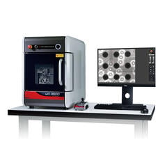
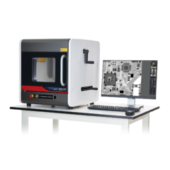
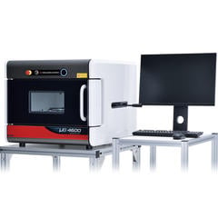
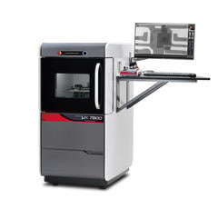
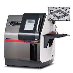
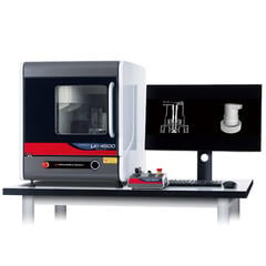
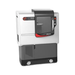
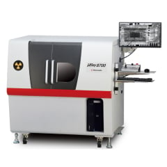
Recommended products
Information on related articles in Technical Knowledge
- Back-End Semiconductor Manufacturing Process
- The Right Way to Choose appropriate X-ray Inspection System
- Principles of Radiography
- How to use X-ray Inspection System safely
- Computed Tomography (CT) Basic and Principle
- Non-Destructive Testing: Types and Applications
- What are X-rays? (Basic Knowledge)
- How to Take a Computed Tomography? - X-Ray NDT series (1) -
- How to View X-ray CT Images - X-ray Non-Destructive Inspection series (2) -
- X-ray Image Processing and Automated Inspection - X-ray Non-Destructive Inspection series (3) -
- What is the difference between Radioactivity, Radiation, and Radioactive Materials?
- Radiation Effects on the Human body and the safety of X-ray equipment


