Scanning Electron Microscopes (SEMs) utilize electron beams with wavelengths significantly shorter than visible light to achieve superior resolution and depth of field compared to conventional optical microscopes.
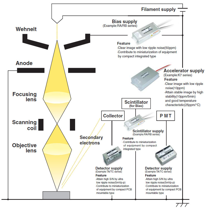
SEMs operate by scanning a specimen in a vacuum with a narrowly focused electron beam. Images are constructed by mapping the intensity of detected signals to the beam's scan coordinates. While images are typically formed using secondary electrons emitted from the specimen's surface, SEMs also detect backscattered electrons, X-rays, and cathodoluminescence. These signals provide critical data regarding surface topography, elemental composition, and electrical properties.
For advanced imaging, Scanning Transmission Electron Microscopes (STEM) utilize transmitted electrons. To further improve resolution--particularly during low-energy imaging--a technique known as beam deceleration (retarding) is employed, where a negative bias voltage is applied to the sample stage.
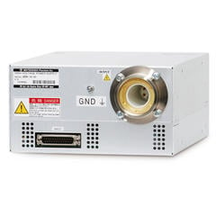
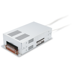
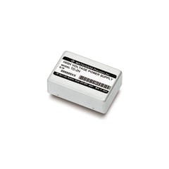
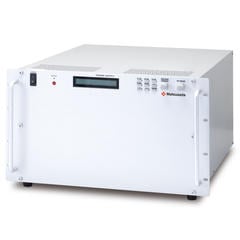
Matsusada Precision provides a comprehensive range of power supply solutions engineered for the demanding requirements of electron microscopy. From the precisionSEM5600 system to specialized high-voltage modules, our products ensure stable performance for acceleration, filament heating, biasing, electrostatic lenses, and detectors.
- Related Terms:
-
- Electron Microscope
- Transmission Electron Microscopes (TEM)
- Electron Beam (E-beam)
- electron gun
- Electron Beam Lithography
- X-ray
- secondary electron
- incident electron
- bias
- Cathodoluminescence
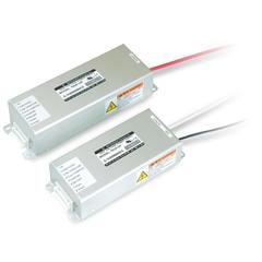
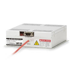
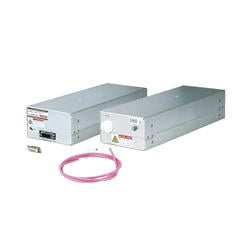
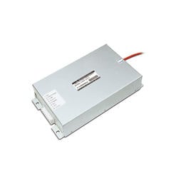
Recommended products
In addition to the PrecisionSEM5600 Scanning Electron Microscope, Matsusada Precision offers a wide array of high-voltage power supplies tailored for microscope components. Our products are optimized for acceleration, filament driving, biasing, lens control, and signal detection, ensuring high reliability and ease of integration.