An electron microscope (EM) uses an accelerated beam of electrons to illuminate a specimen and create a highly magnified image. Unlike conventional optical microscopes that use visible light and glass lenses, electron microscopes operate in a vacuum and manipulate electron beams using electromagnetic lenses.
The wavelength of an electron beam is up to 100,000 times shorter than that of visible light. This significantly shorter wavelength enables superior resolution, making it possible to visualize ultrafine structures and nanomaterials that are impossible to resolve with optical instruments.
Electron microscopes are broadly categorized into two types based on their imaging method: Transmission Electron Microscopes (TEM) and Scanning Electron Microscopes (SEM).
Transmission Electron Microscopes (TEM) transmit an electron beam through a thin specimen. The electrons that pass through interact with the sample and are magnified by electromagnetic lenses to project an image onto a fluorescent screen or digital sensor. TEMs require high accelerating voltages to give electrons the energy needed to penetrate the specimen.
Scanning Electron Microscopes (SEM) scan the surface of a specimen with a finely focused electron beam. The system detects signals--such as secondary or backscattered electrons--emitted from the surface to form an image. This technique provides detailed 3D-like images of surface topography and can be used to analyze elemental composition.
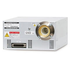
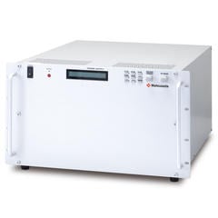
Matsusada Precision manufactures a wide range of high-stability, low-noise power supplies designed for electron microscopy. Our products support critical functions including beam acceleration, filament heating, and lens biasing.

- Related Terms:
-
- Scanning Electron Microscope (SEM)
- Transmission Electron Microscopes (TEM)
- Electron Beam (E-beam)
- Electron Gun
- Electron Beam Lithography
- Electron Optics
Recommended products
We offer specialized power supplies for electron guns, lenses, and detectors. These units can be customized to meet specific OEM requirements.